
There are 3 main kinds of transistors - Bipolar, Junction
Field-Effect (JFETs), and Metal-Oxide semiconductor FETs
(MOSFETs). Both come in N and P varieties with opposite
polarities. This page is mostly about JFETs and compares them to
bipolar transistors to illustrate why JFETs work better for simple
preamp stages. Later on down this page I get into a few
MOSFET-based things I've been working on.
There's a lot of talk about why tubes sound better than
transistors, often attributed to how tubes clip gently and
transistors clip with hard edges. Roughly accurate but there's
more to it than that - transistors don't necessarily clip hard and
tubes can clip with hard edges when pushed. Rather, the main
difference is a tube (and a JFET) is a voltage-driven device
that's fairly linear when biased properly, whereas a transistor is
a current-driven device that tends to be more nonlinear and
usually requires negative feedback to correct, that's where the
hard clipping edges come from, especially in the extreme case of
opamps.
Here's a simple bipolar transistor preamp stage with varying
amounts of drive...


Before clipping it looks ok but the distorted waveform is.. well
yuk. The top of the wave rounds and the bottom squares, and when
distorted the base rectifies the input signal causing the duty
cycle to shift, basically losing power. Some duty cycle shift is
OK but with this circuit it only gets worse the harder it's pushed
and there's no way around it because the base is biased positive
to the emitter, any distortion that causes the emitter to stop
following the input signal turns the base into a diode. The
resistor values are fairly high in this example but reducing all
the resistors by a factor of 10 (and increasing the caps by 10)
makes little difference other than increasing the current drain.
Here's an almost identical circuit using a JFET instead of a
transistor...


Much better! There's still a hint of rounding on the top of the
wave but it's partially because it's not biased perfectly
centered. Compared to the bipolar transistor, the FET stays
cleaner until it reaches clip then it flattens more or less the
same on both sides, and there is no duty cycle shift. Eventually
the gate will conduct and shift the duty cycle but it takes over a
volt of input as the gate is negative to the source, the signal
has to exceed the bias point plus the juction drop before
rectification can occur. Tubes do a similar thing (to a greater
extent as the signal voltage vs rectification voltage is greater)
but the solution is the same - add some resistance between the
output of a stage and the gate of the next stage (or in series
with the gate) so if the gate conducts at least it won't load the
previous stage and cause further issues. But keep in mind that
resistors are noise makers by the laws of the universe, use only
as many ohms as needed.
The 2N4393 shown in the simulation is available but the common
J113 has practically identical specs (Vgs threshold from -0.5V to
-3.0V) and works about the same in this circuit. To minimize
unit-unit variation I made the source resistor the same as the
drain resistor, typically the source biases about 1.3V above the
gate with a typical variation of +/- 0.4V (but not guaranteed!),
because the source and drain resistors are the same value this
limits the drain bias shift to the same amount. There will be some
unit-unit variation but it's less than in typical JFET example
circuits that omit R3 and use a smaller resistor for R4, those
circuits usually require a trimmer for R4. The gain is determined
roughly by R6 divided by the parallel combination of R4 and R5
(minus a bit) so if R4 is a trimmer it's going to also change the
gain (and also the output level). Also note that dialing up more
gain by reducing R5 increases the clean distortion and causes more
pre-clip rounding on the top side of the wave. Biasing the gate
positive with a larger source resistor limits the output swing but
it's worth it to reduce variability, and if trimming is needed it
can be done using R3 or R4 with less gain variation. It also
simplifies the design process - whatever the supply voltage is,
divide it by 3 and bias the gate to that voltage minus the FET's
typical operating gate voltage, which for the J113 is about 1.3V.
So 1.6V on the gate results in 2.9V on the source, 2.9V across the
drain resistor and 3.1V across the FET, in the ballpark. It's a
bit more complicated than that, the source follows the signal
(unless R5 is 0) so the bottom clip point gets pushed up by the
signal on the source - so having a bit more voltage across the FET
is a good thing - but there's also loading effects which tends to
need less voltage across the FET to balance out the clipping.
Now to analyze the distortion characteristics using FFT plots.
Before distortion there isn't much difference...


For both the transistor and the FET the 2nd harmonic is about
32db down, or roughly 2% distortion, the other harmonics fall off
about the same. Running clean both these circuits will sound about
the same - transistors can be "warm" sounding, at least much
better than chips.
Running the circuits into clipping better shows the difference...


Besides the FET waveform looking better, the higher harmonics
drop off more rapidly. The transistor's spectrum looks harsh and
this is fairly mild clipping.
Here are the LTspice (version 4) files for the above
simulations...
transistor.asc.txt - the basic
bipolar circuit
transistor1.asc.txt - modified
for FFT analysis
tfet.asc.txt - the basic JFET circuit
tfet1.asc.txt - modified for FFT
(remove the .txt extension or copy to an .asc file)
LTspice is available from Linear
Technology's software page, I use version 4 (under wine) but
a newer version is available. Simulation isn't perfect but for
what it does it's almost like magic. Just keep in mind that it
doesn't model parasitic effects from the circuit layout and the
components are assumed to be perfect unless otherwise specified.
Usually if a circuit works in LTspice it'll work in the real world
although sometimes it might need a few tweaks to compensate for
effects that are not modeled. For audio usually the simulation is
spot-on.
A 3-way Tone Network using a
JFET
Disclaimer - I haven't actually built this circuit... it "should"
work pretty much like the simulation but the component values in
the tone network will likely need "by ear" adjustment depending on
the application.
This circuit implements a 3-band cut/boost-type tone control
network using a JFET for the gain stage. With the controls
centered the gain is roughly unity (minus about a db). The bass
control (on top) has a range of about +/-10db at 80hz (more at
lower frequencies), the mid control has a range of about +/-7db at
1khz, and the treble control has a range of about +/-10db at 7khz
(more at higher frequencies). This type of tone network probably
wouldn't make for good guitar amp tones by themselves (too flat,
guitar amps typically scoop the mids), the application I had in
mind is putting it after an overdrive circuit that's already
equalized to sound about right to allow better control over the
overdrive tone.
The circuit has a fairly low input impedance (about 15K) that
varies with frequency so it should be driven from a low impedance
source. For high impedance sources use a buffer such as this
circuit...
              .----------*------< 9V
              |          |
             2.2M        |
              |      |---'
in >--0.01u---*----->|  J113
              |      |---.
              |          |
              |          *---1u---> to EQ
             1.8M        |
              |         10K
             _|_        _|_
Because the circuit cuts and boosts, keep the input level fairly
low (around 100mV RMS) to avoid clipping at extreme settings. The
circuit has a fairly low output impedance (about 5K) but if
driving an input with an impedance of less than 100K increase the
size of C7 to avoid bass loss.
Here's the circuit response with the tones flat and driven
slightly into clipping...

Maximum undistorted output is roughly 1.7V RMS, FET variation
might reduce this somewhat if not biased perfectly centered. The
bottom bias resistor is slightly bigger than the previous examples
because the higher current means less gate-source voltage
difference and also because the source resistor is fully bypassed
so it won't be going up and down with the signal. Note how the
gate signal is distorted as the feedback corrects the distortion
of this configuration. Controls U1 to U3 are 300K linear-taper
controls, 250K linear controls should also work OK. In the
simulation the controls ended up being backwards, wiper=0 for all
the way up and 1 for all the way down, the correct orientation is
for the wiper to travel to the left (towards the input) as the
control is increased.
C4 sets the bass control frequency, C6 sets the mid control lower
frequency, C5 sets the mid control high frequency, and C2 and C3
control the treble control frequency (could just be a single
capacitor in series with R10 but this arrangement permits setting
the cut and boost frequencies separately). R5 and R6 set the bass
control range, R8 and R7 set the mid control range, R10 sets the
treble control range. R9 is fairly large compared to the other
resistors to minimize interaction.
Here are AC response plots for various control positions. Flat
and with the bass control 90% up (sim wiper setting at 0.1)...


Bass at 10%, mid at 90%...


Mid at 10%, treble at 90%...


Treble at 10%, the last plot is with the bass at 90%, the mid at
10% and the treble at 80%...


Here's the tonecb_ac.asc.txt
simulation file and the potentiometer
model it needs to run.
An Old-Style Guitar Preamp using
JFETs
This is similar to the preamp used in ShoBud amps with more of a
rock-n-roll twist - I used a 50K mid control (with an extra
capacitor) instead of the usual 10K, and added a master volume
between the 2nd stage FET and the output buffer. The original
ShoBud preamp had no master and the base of the output buffer
transistor (a regular bipolar NPN) connected directly to the drain
of the 2nd stage, an arrangement that wasn't designed to be
clipped. Although provisions are made to let it get a bit dirty,
it's not an overdrive preamp and is more like the clean channel of
a typical tube amp. The output of the circuit can be run into any
typical power amplifier that needs a volt or less for full output.
Or run through a reverb circuit or an effects loop first. This is
another circuit I've only "built" in simulation in this exact form
but I've used variations of this many times over the last decades
and it sounds very much like a tube amp.
Here's the circuit running clean and clipped...


The circuit runs at 18V, the simulation schematic shows 50V
because that's what's typically available from the power amp
section, reduce R20 if running from a lower voltage to ensure that
the zener diode conducts and properly regulates the supply. The
simulation shows 2N4393 but almost any N-channel JFET with a
reasonably low Vgs threshold should work - J113, MPF102, 2N5457
etc. If clipping is off-centered tweak the values of R5 and R12
(with a J113 model I needed 75K for symmetrical clipping). R6 and
R13 set the gains of the first and second stages, reduce for more
gain. I configured the first stage has less gain to avoid
overloading the input stage.
The tones resemble a normal guitar amp tone stack but I used
somewhat different capacitor values, made the mid control bigger
to make it more useful for boosting the gain. The extra capacitor
C13 keeps it from boosting the highs along with the mids. C6 and
R9 add a high treble boost at lower volume settings, R9 controls
how much brightness is added. R9 is often a switch for full
bright. The simulation shows some rolloff above 8khz, not sure
what's up with that since there are no added high-cut caps
(probably the "miller" capacitance of the 2nd FET). Guitar
speakers cut off around 7khz so it doesn't matter much but this
might be one of those areas where simulation deviates from
reality.
Here's the AC response with the controls centered (20% log
controls)...

The following plots show the response with the treble, mid and
bass each at 10% and 90% with the others centered...


Something resembling flat is obtained with the treble at 50%, the
mid all the way up and the bass at 20%...

Here's the fetgpre_ac.asc.txt
LTspice simulation file, requires the potentiometer_standard model.
Dealing
with unit-to-unit variation
JFETs have very loose specs when it comes to gate threshold, for
a 1uA threshold the J113 has a specified Vgs from -0.5V to -3.0V.
Other units are no better, it's just something the designer has to
deal with when using JFETs. Biasing the gate positive and using a
big source resistor helps (in that the circuit will usually work)
but it does not eliminate the variability, especially when running
from 9V as with a guitar pedal.
Here's a J113 model that can be used with LTspice to explore the
effect of varying gate thresholds...
.MODEL J113 NJF (VTO=-1.29 BETA=9.25964E-003
+ LAMBDA=3.03839E-002 RD=1.30170 RS=1.30170 IS=9.86870E-016
+ CGS=1.05000E-011 CGD=1.20000E-011 PB=5.04493E-001 FC=0.5)
To use this model select the text icon and select spice
directive, paste the above text into the text box and place
anywhere on the schematic, then the 2N4393 text can be changed to
J113 (right-click and change the part label text itself, it won't
show up in the part select dialog). The default VTO is -1.29 but
this can be changed to explore the effects of variability.
Here's the simple preamp circuit with the default threshold...

Here's the waveforms with the VTO=-0.9 and with VTO=-1.7 (about
+/- 0.4V)...


...yea that's a problem. Both will "work" but will sound
different.
Here's the guitar preamp with the J113 model (source resistors
changed from 82K to 75K)...

Here's the response with VTO=-0.9V and VTO=-1.7V...


...not as bad because it's running at twice the supply voltage,
but still some variation.
So what to do? One thing that can be done is replace the source
resistors with trimmers, especially the last stage where the
effect is most noticeable. But that adds cost and there's the
additional labor step of connecting it to a signal generator and
scope to make the adjustment. Another way to compensate is to
grade the FETs - Here's a test circuit that replicates the bias of
a preamp circuit...
         G O-----------*---2.2M----------.
   FET                 |                 |
  under  D O-----------|----*----47K-----*------O +
   test                |    |            |        9V battery
         S O--47K--.  470K  `-> -    + <-'   .--O -
                   |   |       to meter      |
                   `---*---------------------'
Since the source and drain resistors are the same, for proper
unloaded response the meter should read about 3V, but typically
you'll need a bit more voltage to account for loading effects,
3.1V or so with a 150K load. Regardless go through a bunch of FETs
to see what the average is then in your circuit size the top bias
resistor (or the source resistor) to produce the desired clip
characteristics. Mark all the FETs close to the average say
yellow, these are the "good" ones. If the meter reading is less
the FET draws less current, paint it green and to optimize it use
a smaller resistor for the top bias resistor. If the meter reading
is greater paint it red and use a bigger resistor to optimize. Or
just use the yellow ones for the last stage and put the reds and
greens earlier in the preamp where exact clipping symettry isn't
an issue.
Using JFETs
for Guitar Overdrive
My preference is real-tube overdrive, but JFETs do sound quite
nice when overdriven and because of how they work can be dropped
into circuits that resemble actual overdrive amplifier preamps.
The following is a recent variation of a circuit I've been using
for years (actually about three decades), and other than using
JFETs running at low voltage, is fairly similar to the tube amp
mods I was doing back in the late '80's and early '90's at Shiloh
Music and outlined in my Amp Mods document. Basically it's a
3-stage overdrive with a compensated gain (when low boosts highs,
when high cuts lows) between the first and second stage, a fixed
shelving low-cut filter between the second and third stage,
followed by passive high filtering and a kind of funny 3-way tone
network, the volume control and a unity gain buffer. Here's the
basic circuit showing waveforms at various points...

Other than the tone control network and stage details, it is
similar to the overdrive circuits I was making in the '90's and
ever since. Besides using JFETs running at low voltage, the
biggest difference between this circuit and my old tube amp mods
is biasing the gates somewhat positive to allow using large source
resistors to minimize unit-to-unit variation as previously
discussed, thus it requires extra coupling capacitors. Some of my
older JFET versions had ground-referenced gates but that meant
having to use source trimmers and adjusting each stage, that got
old.
Omit C1, C6, R4, R12, R19 and the gain-dropping resistors in series with the bypass capacitors (tube amps need more gain to get to the hundreds of volts needed to clip) then the circuit is almost identical to my overdrive tube preamps, which are in turn similar to something like a JCM800 master volume amp with the bypass caps stuffed and a few caps added to tone down the highs. It's all an evolution of tone!
So what makes this circuit good? As a guitar player I'm very
picky about my tone - I want "clean" overdrive where if I back off
my guitar volume it cleans up, doesn't get harsh when I push it,
gives me lots of gain to get that magical harmonic feedback, and
not mud out when I play chords... I want to hear every note of the
chord no matter how high the gain is cranked. The secret to
achieving this is related to physics.. sonically it sounds like
all the notes on a guitar are about the same volume, and
energy-wise they are. But clipping is about amplitude and that's
not energy, to sound the same volume a note that's half the
frequency requires twice the amplitude, and that's why many
overdrives mud out - a flat preamp will clip the low notes before
the high notes and that's no good because then you can't play
chords without the lows overpowering the highs. Even worse, if
flat after the clipping stage it'll sound harse, even
smooth-clipping devices like JFETs and tubes create too many high
harmonics. The basic trick isn't that hard - cut the lows and
boost the highs before the clip stage, then boost the lows and cut
the highs afterwards. That way the low and high notes have roughly
the same amplitudes so they clip together instead of clashing, the
high cut afterwards gets rid of the mosquito sound, and the low
boost afterwards restores the lows that had to be cut before the
clip to keep it from mudding out. If done right, when not clipping
the frequency response is fairly flat with plenty of highs despite
the harmonic filtering, and when driven it's nice and smooth with
roughly the same harmonic content.
That's the basic idea but there are other tricks. Guitars
(particularly those with single-coil pickups) output a significant
amount of signal above the normal hearing range (ultrasonic), this
needs to be filtered out or else those inaudible signals will
distort together and make ugly sounds. That's what causes
"spatter" when picking high notes hard through some overdrives,
that static-like sound that cleans up when the guitar's tone
control is backed off. Fixing that is usually as simple as adding
low-value capacitors to the gain stages to limit their gain at
very high frequencies. Another trick is the compensated gain - the
amount of low-cut and high-boost depends on how much gain is
applied, if the pre-clip EQ was fixed then at low gain it would
sound thin and at high gain it would sound harsh and cause
high-frequency feedback issues (squeal). So the gain control is
designed to cut more lows at higher gains, and boost more highs at
lower gains. Basically, it's a medium-value capacitor feeding the
gain control, a resistor from the wiper to the ground, and a
small-value "treble bleed" capacitor in series with a resistor
from the control hot to the wiper. The feed capacitor is chosen so
at lower gains there's sufficient low-end response and at higher
gains the resistor from the wiper to ground causes more low
rolloff. The bleed capacitor value is chosen so that at low gains
it produces enough treble boost to counteract the harmonic filters
after the clip stage, the resistor in series limits the amount of
treble boost. These 4 components define the pre-clip EQ at
different gain settings, usually I select them by ear to get the
response I want.
The fixed mid/high boost between the 2nd and 3rd stages helps to keep the overdriven tone tight and focused, especially at high gain settings where the 2nd stage also clips. R16 sets the amount of low-frequency attenuation, C10 sets the turnover frequency, C7 sets the lower low-frequency limit under which lows are rolled off without shelving. If desired R16 can be replaced with a "focus" control to vary the amount of low frequency attenuation, a 1M control varies the attenuation from none to about 9db. This is about the same circuit found in the JCM800 master volume amp and other similar designs.
Another undesirable effect is if the signal forward-biases the
tube grid or JFET gate it acts like a diode and both shifts the
bias point and loads down the previous stage. This isn't as big of
an issue with JFETs as with tubes due to the lower voltages but
the fix is the same.. put some resistance in series with the gate
or grid. That doesn't do much for the bias shift of the stage
being driven but it helps control the loading effect, which can be
worse (essentially shorting the output above a certain voltage). A
bit of bias shift under duress sounds good, gives it that "it's
about to blow" sound, vary R10 and R18 as desired or omit. The
resistors also serve another purpose - miller effect, which
attenuates high frequencies. With tube amps sometimes I have to
take additional measures besides the series grid resistors - EL34
amps in particular are quite sensitive to being fed an
asymmetrical signal under overload conditions - the wires in the
tubes often light up cherry red on one side! to fix that have to
add diodes to counteract the bias shift.
Clipping symmetry is controlled by R17, R19 and R21 which
determine the 3rd stage bias point, the values are chosen to clip
on both sides roughly at the same time for near-symmetrical
clipping. I've never been a fan of asymmetrical/uneven clipping,
(besides potentially blowing up EL34 tube amps at high volume) to
me it just doesn't sound right, like one of the output tubes is
blown. But to each their own, harmonica players love uneven
clipping and many popular distortion designs use that technique, I
suppose because it increases the 2nd harmonic. If that's your
thing R17 can be replaced with a 1M linear taper control or
trimmer but expect it to make static noise when adjusted, controls
don't like DC on them.
With the core overdrive stages tamed, now have to add a post clip
filter network to keep the harmonics under control and provide
tone controls to balance the tone when switching between clean and
dirty. In this circuit the harmonics filtering is done by C13, C21
and C22. Note that capacitors placed directly on a stage output
(drain or plate before or after a coupling cap) have a different
effect than capacitors with resistance between the stage output
and the capacitor - when placed directly on a stage output then
the effect of the capacitor is modulated by the high/low output
voltage excursion and produce much more filtering on the high part
of the waveform than on the low part because when high the output
impedance equals the drain resistance and when low the output
impedance is near zero (whatever the source gain-setting resistor
is). This effect is greater with JFETs than with tubes, which
don't pull all the way low. For the very-high-frequency filters on
the 1st and 2nd stages this doesn't matter much because those
stages aren't clipping as much but definitely makes a difference
on the final clip stage. In this design C13 is the one that mostly
shows the effect (and is small enough to not matter), C21 is
affected but only over a 2-1 frequency range, and C22 and the
tones have no asymmetrical filtering effect at all.
The low control provides a low-cut when turned down, and when
increased blends in a capacitor to provide bass boost. The high
control is similar to a guitar tone control, and the mid control
is kind of like a mild notch filter. The controls don't have a
great deal of range because I wanted a pedal that sounded OK with
just about any setting (I don't like having to "find" the tone)
but still had enough range to balance with the bypass sound and
compliment the amp tones. There are a huge variety of tone control
circuits that can be substituted here, including the 3-band active
EQ circuit presented earlier.
Here's an animated GIF of a similar circuit showing transient
waveforms and frequency response as the controls are adjusted...

The waveforms are similar to what I get from a tube amp with a
similar design.
I reflected a bit before posting this overdrive design as it's
similar to an overdrive pedal I've been making at Superior Music.
But frankly it's not getting much exposure and love lately so I
feel the need to explain why this design rocks, and to do that I
need to reference actual circuits or it's mostly just a bunch of
marketing hand-waving. This makes it real, it can be built and
verified. I do need to record some clips of playing through it but
if you've heard
me play live
or heard one of my amp mods, it sounds kind of like that. However
- sound clips don't convey how it feels - with designs like this the player can
control how it sounds by how the notes are played.. soften up and
it cleans up, closer to the bridge for higher harmonics, play a
5/1 inversion and it generates an octave-down subtone that sounds
like a monster chord, use your palm lightly to generate high
harmonics or more damped near the bridge to accentuate the bass.
This design doesn't sound exactly like my tube amp designs (after
all it ain't hot tubes!) but JFETs are similar enough to tubes to
be able to use the same general principles to achieve a similar
effect.
Some of my amp mods for
comparison
Here are a few of the tube amp mods I've done over the years...


The first design is the modified Fender Princeton I've played
through for years - since drawing that schematic I added a
transistor unity-gain buffer (emitter follower) between the master
volume and effects send jack to avoid loosing highs when using
with a pedalboard. It doesn't really have clean/dirty switching,
in "lead" mode it boosts the gain of the second stage and inserts
a level drop and extra filtering after the third stage. The gain
control has low-cut compensation but no "treble bleed" because
that would make it too bright in clean mode. For the same reason
it doesn't have the mid-high boost between the 2nd and 3rd stages,
just a simpler low-frequency rolloff. Despite that, the JFET
overdrive sounds more like this amp than not.. in fact one of the
reasons I made this thing was so that I could get the sound I
liked from just about any amp.
The remaining mods more closely resemble the 3-stage JFET OD
circuit with variations. For the 75 mod had to figure out what to
do with all those pull switches. The Bassman mod doesn't show a
treble-bleed network but ended up adding one later then the
customer brought it in for adjustments - besides that put the
clean gain before the overdrive gain to make it easier to dial in
mild overdrive (not everyone likes balls to the walls) and added
"speaker emulation" filtering to the line out. The Bandmaster mod
is close to the JFET OD design until it gets to the tones. Both
the Bandmaster and Bassman mods have interesting tone networks I
would mind trying again in a pedal design. The component values
for the various elements vary quite a bit, when I do a mod (or a
new pedal design) I'll start out with the basic topology then
tweak it by ear until it sounds the way I want.
More JFET Overdrive Stuff
Here's an older version of the 3-stage JFET overdrive design, and
something I haven't had a chance to make (yet)...


The 8-3-16 version is simpler and more closely resembles the tube
amp designs from which it came from. I wasn't crazy about how the
low control worked - it could only cut lows, not boost them - and
it had asymmetrical harmonic filtering so kind of had an edge to
it. The latter issue (if it is an issue, tube amps do that all the
time) can be addressed by lowering the value of the 1000p on the
stage 3 drain and adding another small-value capacitor after the
47K to ground. Fixing the low control is trickier but could
increase the value of the 0.01uF coupling capacitor to say 0.033uF
to 0.1uF, adding a 100K resistor in series with it, changing the
22K to 47K then adding a 0.0022uF capacitor in parallel with the
low control, then it would more resemble the later design.
The dark blue design is... interesting. Starts off with a normal
JFET preamp and compensated gain control, a low-cut "focus"
control, then it gets a bit different. The stacked JFET's are what
is called a "mu-amp", or at least my take on it. The original
circuit was published in the '70's in the app note AN-32 by
National Semiconductor but it used parts that are no longer
available, if made as-is with modern JFETs you get a circuit that
draws ~10ma and has poor gain. Crafters soon realized they had to
insert a resistor in the bottom JFET source to bias it, then
bypass it with a capacitor. With that (obvious) mod the circuit
works fairly well and was used by several boost and distortion
effects. But there were still a few issues. If the ratio of the
resistors biasing the top JFET gate were equal then the clipping
was asymmetrical (fixable by making the bottom resistor smaller),
it depended on the gate threshold of the top JFET which varies
widely (my more normal JFET circuits mostly compensate for this..
there's no compensation here), the clip symmetry varies with
battery voltage (which happens with normal JFET circuits to but
would like to fix that), and the top and bottom sides of the
output waveform varied a bit too much for my liking, both in shape
and effective output impedance. Normally varying output impedance
isn't much of an issue (pretty much all single-ended preamp
circuits do that) but becomes an issue because the output
impedance of a mu-amp is very high to begin with.
So I tweaked the circuit under simulation.. made the source
circuits of the top and bottom JFETs the same (including the
bypass networks), that pretty much fixed the issues I had with the
circuit - made it more balanced (including top/bottom output
impedance) and insensitive to JFET variation so long as the two
stacked JFETs were reasonably matched with one another, and
insensitive to the supply voltage. Then I noticed something
cool... normally the "bootstrap" cap - the 10uF ceramic connected
to the top JFET gate - would be connected to the drain of the
bottom JFET. When it is the circuit is mostly perfect.. maybe a
bit too perfect. When the bootstrap cap is connected to the top
JFET source instead it does an interesting thing - it breaths!
When overloaded the initial waveform is clean and symetrical but
as the overload continues the clipping symmetry shifts over the
course of several hundred milliseconds. The 47uF values determine
the time it takes for the shift to occur, and the 10uF bootstrap
determines how quickly the top JFET keeps up with what the bottom
JFET is doing, so the value determines how pronounced the effect
is. With 10uF or more it's quite noticeable, with 1uF it only
happens a little, and with 0.1uF there is no shift at all. Does
other interesting things when the values of the 47uF capacitors
are different. This could be put on a switch but better hide it
because if flipped it'll make a loud pop.
The mu-amp stage must be followed by an emitter follower or
anything connected to it will load it down. This is a convenient
place to put a 12db-octave low-pass filter to attenuate the buzzy
clipping harmonics, now made easier thanks to the mods. This is
the classic "Sallen-key" active filter circuit, which is usually
made with an opamp in follower mode but works the same with an
emitter follower. The filter is a bit underdamped to give a bit of
a presence boost before taking the dive, for smoother filtering
change the 100pF to 220pF. The rest of the circuit is a simple
low/high tone control network, the volume and a buffer to drive
the output.
Other than playing with the mu-amp stage and tones under
simulation, I have not tried this circuit, no idea how it will
sound. It will likely require tweaks to the component values
around the gain and focus controls and tone controls. It's
something I scribbled down a few years ago then lost interest in
it after reading stuff about some company laying claim to the
circuit (which I can't find any reference to anymore, they must
have figured it out). It's not an original idea, if you look
around the net there are several others doing similar things, this
is my interpretation of it.
...update... I did make something like the Dark Blue in real
life... have a Purple Cow...

[7/5/25 LOL just noticed the battery is drawn backwards]
Here's what the insides look like...

It's an oddball but it sounds very nice and it has the dynamics
hinted by the simulation - besides a momentary duty cycle shift
(the breathing), after heavy overdrive it takes a bit to
recover...

Turns out the top 470 ohm resistor (R14 in the simulation) has a
lot to do with this, making it around 12K almost eliminates the
recovery effect but I'm not inclined to "fix" it, it acts very
much like a tube amp when abruptly going from heavy overload to
clean. The 2.2uF bootstrap capacitor (C11 in the simulation) also
affects the feel, larger values take longer to recover.
A LM386-based Mini-Amplifier with a JFET Preamp
The LM386 is a popular chip for mini-amplifiers, for good reason - it's cheap, available, easy-to-use and puts out over half a watt into 8 ohms when running from a 9V battery. Here's a LM386 project from ElectroSmash that uses a JFET preamp, numerous other LM386-based amplifiers with JFET preamps are on the net. Here's something I threw together recently...

I drew that from memory after the fact (it's at the shop), should
be close. It started as a hobby kit that included basically just
the bottom half of the circuit with an 1/8" input, volume control
and a (rather tiny) speaker. I added the preamp section with gain
and tone controls and external speaker and power jacks. I made the
amp circuit according to the schematic that came with the kit, it
didn't have the 10 ohm resistor and 0.047uF capacitor on the
output and the plus input (pin 3) was grounded. Worked like that
but probably should add the extra parts - the R/C on the output
helps avoid oscillation and the extra 0.1uF cap on the unused
input should improve output offset.. the original circuit has an
extra ~12.5mV*20=250mV offset from the input resistance,
potentially taking away from the output power. Did notice it
clipped a bit extra on the low side, will try it with and without
the extra 0.1uF cap and use whichever gives the best headroom. Or
could omit the caps.. ground one input and wire the other directly
to the volume wiper. I noticed no oscillation without the output
"Zobel" network but it's on just about every LM386 app schematic
and doesn't hurt. The amp was hooked up inverting because that's
what the schematic in the kit said and the inverting configuration
is more stable (especially with a high gain non-inverting preamp),
for a non-inverting power amp reverse pins 2 and 3 but make sure
the speaker wires are well away from the input jack wires.
The 1N4001 diode on the power jack protects against reverse
polarity by shorting the supply (ouch!) if backwards (but didn't
want to waste a diode drop just for that). The LED should be a
high-brightness type so a 10K series resistor can be used to
minimize current drain. The LM386 draws about 4.3ma at idle, about
0.7ma for the LED and the preamp section draws about 0.5ma, so
about 5.5ma idle current - not much but still don't want to forget
to turn it off if running from a battery. Current consumption when
delivering power is much higher.. roughly idle plus
square_root(output_power/load_impedance)/2 [edit, forgot the /2
part, single-ended] plus losses, for 0.6W into 8 ohms that's about
140ma average. Power into 16 ohms is somewhat less, about 0.4W,
but that brings the peak current down to around 80ma, probably
better if powering from a 9V rectangular battery.
The 2-stage preamp isn't as crunchy as my 3-stage designs but
still distorts quite a bit when the gain is cranked. The stages
are mostly self-biasing to avoid drastic unit-unit differences but
there is still some, vary the 2.2meg high-side gate resistors to
adjust the operating point if needed. 47K resistors are used for
both the source and drain resistors, so for even clipping at 9V
there should be a ~3V drop across the source resistor. The J113
has a gate threshold of -0.5 to -3V, 2.2meg and 470K puts about
1.58V on the gate, for a typical -1.3V to -1.5V threshold that
puts close to 3V on the source, thus about 6V on the drain but
it's not guaranteed over the entire Vgst range. If building get
extra JFETs or be prepared to trim the 2.2meg resistors (reduce to
say 1.8M if much less than 3V across the 47K's, increase to say
2.7M if much more than 3V) but this scheme works out better than
always having to trim. These calculations are for a 9V supply, the
2.2K resistor drops it a bit but at these low currents not much -
at ~0.06ma per fet that's a drop of about 0.26V, not enough to
matter much. Compared to other designers I tend to run the JFET's
"starved" and close to the threshold, this basically takes Idss
out of the equation. The ElectroSmash article details some
alternate approaches with names like "The Tillman Amplifier" and
"The Fetzer Valve", those "circuits" (different combinations of
source and drain resistors with 0V on the gate) are for the J201
JFET which has a much lower typical gate threshold but these days
is only available in a SMT package, the biased gate approach works
with the more common J113 or if you can find them MPF102 or
2N5457. Note that on the TO92 J113 the gate pin is on the right
side looking at the flat spot. Source and drain can be
interchanged which I usually do for layout purposes.
The 2.2K resistor in series with the 10uF bypass cap sets the
gain of the first stage to roughly 20, if optimally biased for
even clipping (about 2Vrms max output) that puts the input
overload point at about 100mVrms for a reasonable chance of being
able to set for clean. Increase the 2.2K value for less gain and
more overload resistance. The 220pF capacitor across the drain
resistor limits the gain at very high frequencies and helps avoid
"spatter" when picking hard with single-coil pickups. The gain
control is compensated so that at low settings it boosts the highs
to make up for the high-cut of the tone control and clip filter,
and at high settings cuts the bass to keep from mudding out. Mess
around with the values of the 470pF and two 220K resistors to
adjust the compensation curve, wired these parts off board right
across the control for easy changes. The second stage is run
flat-out (no resistor in series with the source bypass cap) to
maximize gain, not the best for low distortion but it's a half
watt baby amp, low distortion is not really a design goal. The
drain output of the 2nd stage passes through a 47K/470pF filter to
the output emitter follower, which can be just about any
small-signal NPN transistor - 2N3904, 2N2222 etc (used the first
thing I found don't recall what it was). The tone control is also
connected to this point and for the prototype was simply a 0.01uF
capacitor in series with a pot, works more like a shelving
low/high control than a treble control. Probably can be improved,
see the simulations for a circuit that doesn't cut quite as much
highs when all the way down. I think I used a 22K emitter resistor
and output resistor, the amp only needs about 0.2V for full output
so the output resistor drops the signal so that below about 60%
it's all JFET distortion and can clean up over 60%. I wired the
1/8" jack input after the volume so that it would also function as
a preamp output if needed and also to better mix the guitar signal
with a headphone out, vary the 33K resistors as needed.
I made a LTspice simulation of the preamp to play around with...


The stages are about the same but used a somewhat different tone
control network.. added a 15K and 2200pF in parallel in series
with the existing 0.01uF so that when all the way down it doesn't
remove as much of the high-end while still providing a useful
low-end boost, and added another 2200pF on the JFET drain for
additional options.. can be an extra high control, or if crossed
to the other control, a high boost. Note that the effect of the
drain cap is asymmetric - because the impedance is high when the
wave point is high, as a cut it cuts more of the top side of the
wave, and as a boost it boosts more of the bottom side of the
wave. Haven't tried this circuit but thinking that the drain high
cut and boost resistors (R18 and R24 on the simulation schematic)
can be fixed or trimmers to give the main tone (R19) a greater
range of control, but still get out of the way (leaving mostly a
square wave) when the tone is maxed.
Optimizing the LM386
The mini-amp worked ok but the clipping wasn't symmetrical.
Played around with a LM386 simulation I found and it suggested I
needed to bias the -in pin slightly positive.. when I got back to
the shop and did the mod it made it worse. Took a few measurements
and soon discovered why.. with the original circuit (+in grounded,
-in cap coupled) the output pin was sitting at 3.79V rather than
the expected 4.4V or so (supply was about 8.8V), biasing -in just
drove it lower. Adding the capacitor to the +in pin didn't help
much, just brought it up to 3.85V (was expecting a larger effect).
Biasing was the answer, but had to bias the +in pin instead to
bring the voltage up to about mid-supply. Here are the research
notes and the present mini-amp circuit...


With biasing got it from 405mW to 605mW before clipping into 8
ohms. No idea if my particular LM386 represents the average, came
in a imported kit so wouldn't surprise me if it was a work-alike
clone, but for now going with it. When I get around to PCB layout
I'll add biasing resistor locations for both the +in and -in pins
so no matter what the particular chip characteristics proper
biasing can be achieved.
I made some changes to the simulated LM386 to better match what I
was seeing...


The first two plots show the output with a 16 ohm load, first
with actual (pulsed) current draw, the second with the filter cap
very large to show the averaged current draw.. about 80ma when
delivering about 400mW. The next two plots show 8 ohm output and
current draw.. about 150ma when delivering a bit more than 600mW.
Here's the cba386_1c.asc LTspice
simulation file.
A 9V Mini Amp with a 1 Watt Discrete Power Amp
The LM386 is handy but it has limited output swing, limiting
undistorted 9V output power to about 0.6W into 8 ohms, and to get
that I had to use biasing tricks that probably vary from brand to
brand or maybe even unit to unit (my sample size was one). Without
tricks I could only get about 0.4W out of a LM386. This version of
a mini guitar amp uses a 7-transistor power amplifier to get a
full watt at clipping with a 9V supply...

I haven't actually built this circuit (yet) - if attempting to
build make sure the output bias current is OK (the transistor
models might vary from real parts), there should be about 0.1mV to
0.5mV average across 0.47 ohm resistors R13 and R15 - if too low
decrease the value of R10 (carefully! if the value is too low the
outputs will be overpowered and overheat), if too high increase
the value of R10. R10 probably should be a 1K resistor in series
with a 1K trimpot. When initially powering up the supply current
should be carefully monitored using a current meter, or at least
put a #47 bulb in series with the supply to avoid damage in case
the bias current is too high - if the bulb lights you're in the
weeds.
This amp circuit achieves near rail-rail output through
bootstrapping - for the positive side the output signal is coupled
through C5 to the junction of R7 and R8, providing above-the-rail
drive and also converting the voltage amp (Q2) load into a
constant current source to greatly increase the open-loop gain. On
the negative side, the bottom half of the drive circuit is
connected to divider R11 and R12 from the post-cap output for
below ground drive. C6 is required for stability, under simulation
it oscillates with 0.01uF but 0.022uF is enough. If C4 is 100pF
then it's stable without C6 but I wouldn't trust it. To save a
transistor it uses a simplified single-transistor input stage
where the inverting input is the emitter, but this requires that
the base be biased to about 0.6V less than the half supply point
minus the voltage drop of R5, or about 3.4V. Green LED D2 in the
input bias network provides a constant 1.6V drop to help keep the
output roughly centered as the supply voltage changes from 6V to
12V.
Here's the odamp5.asc
LTspice file for this circuit.
MOSFET circuits
I haven't done a lot with MOSFETs.. they always made me nervous,
some are so sensitive just looking at them might blow them, or
worse damage the gate but still work then blow later. Fortunately
these days one can get gate-protected MOSFETs that can be handled
without precautions. I've made a few power amps with "HEXFET"
outputs, this is one I made into an old Champ chassis with a two
tube preamp...

...not to be confused with a Fender Super-Champ, that's just what
I called it because it was louder than any other Champ I've ever
heard (and I'm pretty sure at the time I hadn't run into Fender's
original Super-Champ with 2 6V6's or I would have labeled it
something else). At least until I let it be used as a monitor amp
at a gig and they connected too many speakers.. smoke came out and
it ended up getting scrapped for parts. If only I had added a
thermal cutout on it.. power MOSFETs are pretty tough, usually
(with simple current limiting like the zeners I used, not marked
but 6.2V or 7.5V if I recall) they can take a short long enough
for the fuses to blow but they can't survive sustained thermal
overload, if only I had used a cutout.
My favorite MOSFET power amp was one I made back in '81 or so..
it also used IRF132/IRF9132 but used a single JFET as the driver -
a now unobtainium TIS-58, those things could take a 100V or more.
Between the output gates I used a TL431 shunt regulator to set the
bias with a single resistor to the + supply on the other side.
Single-ended power supply, speaker was capacitor-coupled, a
trimpot on the JFET source set the bias to put the output at half
supply. Perhaps the simplest power amp I've ever made. Despite no
negative feedback it sounded great. Replicating that design with
modern parts would require using a higher voltage MOSFET for the
driver (JFETs top out around 30V these days), but I doubt it would
sound as good, MOSFETs usually don't have as nice of a transfer
curve compared to a JFET. Just haven't been that interested in
MOSFETs until recently when I realized that the CD4007 wasn't just
another CMOS logic chip...
CD4007-based Overdrive
The CD4007 is more than just 3 inverters in a package, although
the N-channel and P-channel FET pairs have common gate
connections, only one pair has the drains connected together and
all of the individual sources are brought out to separate pins.
Here's a detailed schematic showing the substrate connections
(slightly doctored to correct connection errors)...

The first pair's sources also connect to the substrates of the
other FETs, so pin 14 should be connected to the highest voltage
and pin 7 should be connected to the lowest voltage. Preferably
stable because substrate voltage variations affect the
characteristics of the other FETs. Otherwise the transistors can
be used individually. Thanks to a fellow pedal hacker I was
corresponding with over pedal mods, I learned about this neat
chip.. noticed that on a DOD FX90 schematic one of the FETs was
being used in isolation (most schematics show only logic
symbols).. hmmm gears start turning, had to look into it and sure
enough it was really a mosfet array with semi-isolated
transistors. Of course the first thing I start thinking is
overdrive pedals. I simulated a few things that at first had me
amazed only to find out my models were inaccurate and when I
plopped in more accurate models the circuits no longer worked..
but with tweaks got it working again. Finally I found Lynn
Fuller's more accurate (I hope!) level
7 CD4007 models and wired up the simulated circuit to at
least partially simulate the parasitic components.
This is one of the circuits I've been playing with in LTspice...

The basic topology is similar to the "Dark Blue" overdrive idea
presented earlier, a preamp stage driving a "mu amp" formed by
stacking a FET on top of another to serve as a current source,
increasing the gain. In this case not as much as the JFET version
due to negative feedback but it still has a maximum gain of about
300 according to the simulation. Disconnecting R13 increases it to
about 500 but then the gain controls won't work right. For this
application I wasn't after lots of gain but was trying to try to
linearize the output stage, I like rounded clipping but the usual
mosfet inverter roundness is a bit too much. I'm still tweaking
but in this circuit but with the present values under simulation
the mu amp stage actually has less gain than the inverter preamp,
but the clipping is more like... clipping. Here's the 4007mudrive1.asc LTspice file.
The following simulations are from a similar earlier version of
the simulation, ignore the "Cascode" in the comments, that was a
mistake - a cascode circuit is a common source amp connected in
series with a common gate amp.. a mu amp is (more or less) a
common source amp with a constant-current load. These simulations
were done before realizing that the NRS and NRD properties were
interfering with the models (the effect was minor for this circuit
but makes much more difference for higher current circuits - more
on that in a bit), and before playing around with the tone
network.
It starts off rounded then flattens...


The top flattens more than the bottom because of the substrate
diodes shorting out the bootstrap, but it's still much better than
the clipped output of the more traditional inverter preamp, the
gray trace in the last image. The drive controls go below unity so
that sound can still be accessed. One of the things I find
interesting about this circuit is (like the JFET version) it has
dynamics...


As the signal is applied the operating point shifts downward
(shown by the brown band showing LED current which is in series
with the output buffer source resistor.. the status LED flickers
while playing:-) causing the clipping to shift towards the bottom
side. Capacitor C2 sets the time constant - these are with 1uF,
0.1uF causes the shift to happen rapidly, 10uF causes the shift to
happen more gradually, this can be a 3-way "feel" switch. There
looks like there would be recovery effects between notes.. after
the signal stops abruptly there's a pretty drastic downward shift
as the bias is sucked out (C2 sets how fast it recovers).
Simulating using a switched signal showed that while there is an
effect it doesn't fully cut out the signal and it fully recovers
within a few cycles. The duty cycle shift has a limit, under heavy
overdrive it squares and stays square, the dynamic effect is
mainly at the transition between clean and clipped.
This thing should be pretty nasty.. anxious to throw together
something to see how it really sounds. The tone network is just an
initial guess and something for the sim, the final circuit will
probably be different.. in an AC response simulation it wasn't
that great. I expect some values will have to be adjusted to work
with a real CD4007 chip. There's nothing really unique about using
the CD4007 as a preamp, once I looked for it I found several
examples on the web, mostly overdrive pedals. There are also
several mu amps using mosfets on the net but didn't see any using
a CD4007, most use 2N7000 or BS170.
Still working on accurate models.. the Lynn Fuller models from
the "Introduction to Modeling MOSFETS in SPICE" document seem
pretty good, but there's a typo in the properties line - omits the
NRD=0.54 property (also it's supposed to be NRS=0.54 not O.54, an
OCR error). These determine the source and drain resistance from
other factors, defaults are 1. In the above sims I omitted the NRD
property in all the mosfets, but adding them back made almost no
difference and omitting both NRD and NRS only causes a relatively
minor bias shift. However, when I tried to simulate the
traditional self-biasing inverter preamp circuit the results
weren't so great.. worked but off center and distorted. In this
case omitting NRD and NRS permitted the circuit to work mostly as
expected, so now wondering how accurate the model is for
simulating analog circuits but being a resistance thing it's
probably something that only comes into play with higher current
circuits. On the other hand, the N-channel and P-channel mosfets
in a CD4007 have different characteristics so I wouldn't expect
them to self-bias perfectly.
I simulated a circuit similar to the most common preamp
application...


The top two plots are with the NRS and NRD properties omitted,
looks about right, self-biases close to half supply. The second
two plots are with NRS=1 and NRD=1 for all the mosfets which
should be identical but quite clearly the default is not 1! Or
more likely the default really is 1 as documented but there's a
bug in how LTspice calculates those properties. The plots for the
recommended Pchan NRS,NRD=0.54 and Nchan NRS,NRD=0.1 are almost
equally bad. It gets worse when using with the simplest circuit
with the sources grounded and at supply, with NRS NRD omitted
versus the recommended values...


Yuck! I don't know for sure until I breadboard the circuit, but
I'm leaning heavily that the first plot is a lot closer to what
it's supposed to look like, at least that's what I remember from
working on Sunn Beta amps which used CMOS inverters as preamps.
Using NRS NRD values of 1 and 0 made little difference. Until I
get to the bottom of it I'll be omitting those properties. I'm
running LTspice under wine which is known to sometimes induce bugs
but usually only with the GUI due to differences between the real
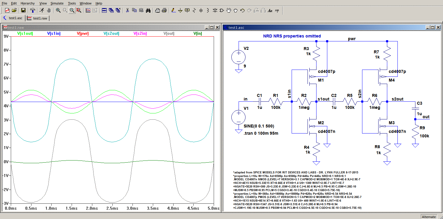
and fake libraries, never seen it bug out on math. Here's the test1.asc LTspice file.
The following simulations test the N-channel and P-channel
mosfets in a very low current common-source amplifier
configuration...


...if actual performance is anything like that then that's great!
The P-channel MOSFET has a bit more edge on the drain side when
hard-clipped but these kinds of circuits are usually done using
the N-channel MOSFETs. The N-channel MOSFET does it too but not
quite as much. Note that the other side of the source bypass cap
for the P-channel MOSFET is grounded to improve supply rejection
but otherwise the two stage configurations are mirror images of
one another. With the values shown the effective input/node
impedance is about 85K, thus stage gain is about
2.2M/(85K+InputR), or about 17 for the first stage and about 7 for
the second stage (not counting the effect of the output impedance
of the first stage).
The circuit works without the source resistors and their bypass
capacitors but then the 2.2meg resistors from gate to source have
to be reduced and tweaked, adding the resistors/capacitors
provides a convenient way to set the stage bias without messing
with the feedback resistors. These plots are with NRS/NRD omitted
but with only 41uA current those properties make little
difference, just a slight gain reduction. Because of the low
operating current these circuits should be a good test of spice
model accuracy. Here's the test8.asc
LTspice file.
A more practical CD4007 overdrive circuit
I like the strange dynamics aspect of the "mu amp" circuit, but
it's a lot of parts and more to go wrong if the actual parts don't
match the models, and unlike other mu-amp variations its "mu-ness"
didn't increase the stage gain all that much (plus was knocking it
back down with negative feedback anyway). Need something simpler
to plan for an actual build. This circuit uses the complimentary
preamp section and the drive and tone controls of the previous
mu-amp design, but the mu-amp itself is replaced by a simple
conventional gain stage. I have seen CD4007-based variations of
both types of circuits in the wild so this one has a fairly good
chance of working...

This schematic shows the input/output/DC jacks, battery and
footswitch needed to make a real pedal. The 2.2K resistors set the
stage biases, these values produce fairly even clipping under
simulation, with a 9V supply (9.6V at DC jack due to the diode)
the bias 1 resistor sets pin 12 to about 4.14V, and the bias 2
resistor sets the voltage at pin 8 to about 4.22V - decrease the
2.2K value to lower the voltage, increase to raise. If not in the
range with ~1K-5K then the 2.2M resistor on the bottom might need
tweaking.. increase to lower the voltage on pin 8, decrease to
raise. The drive and tone control caps are basically guesses, once
made will tweak by ear if the controls don't do what I want.
When using the CD4007 dealing with the substrate connections can
be tricky - note that the unused pins 1-5 are returned to pin 7
(negative substrate) to avoid possible substrate conduction
effects - all pins should at or greater than Vss and in this
circuit Vss sits at about 0.3V. Unused pin 13 is connected to pin
14 since the drain of that FET is connected to 14, grounding would
cause unwanted current flow. The source of the first stage rests
at about 1.5V and doesn't dip under 0.9V even with high input
level (at least under simulation) so that shouldn't be an issue
with this circuit, but in general the FETs should be chosen so
that pin 7 is the lowest voltage and pin 14 is the highest
voltage. Also keep in mind that any signal present on pin 7 or pin
14 gets fed back to the substrates of the other N and P channel
FETs, changing their characteristics and potentially causing a
feedback loop.
This isn't a particularly high gain overdrive, with the drives
cranked under simulation it starts getting into the dirt with an
input of around 6.5mV or so. For more saturation clipping diodes
can be connected at the input of the tone network, the schematic
shows a couple ideas using a DPDT center off toggle switch to
select symmetric, none, or asymmetric clipping. Asymmetric
clipping produces DC offset so the circuit includes a capacitor in
series with the diode along with a normalizing resistor to
minimize the effect. The value of the capacitor affects the
dynamics and low frequency clipping response, in the circuit shown
connected the capacitor is connected all the time for both
symmetric and asymmetric selections, the alt circuit on the bottom
connects the capacitor only for asymmetric clipping. Note that
when using the diodes the output level is drastically reduced, to
avoid surprises the switch should be positioned to minimize the
chance of accidentally flipping.
With no diodes connected and the drive controls at minimum (max
resistance) the output stage doesn't clip and the input stage
starts clipping around 35mV with the classic CMOS inverter
roundness. The drive controls are 3meg reverse-audio taper, what
was for the old Fender tremolo speed control and readily available
from amp parts suppliers. The idea behind two drive controls is
the low drive has a lower high-pass frequency, so it can be set
lower and the high drive cranked to bypass it more at mid and high
frequencies for more bite and to make up for the treble cut after
the clipping stage. Will see how that works out.. could use a
single "compensated" gain but the dual drives should provide more
control over the pre-clip EQ.
Here are some simulations of the circuit without the saturation
diodes...


The following simulations show the effect of the extra diodes in
asymmetric and symmetric configurations...


In this circuit the difference between symmetrical and
asymmetrical diodes is subtle due to the DC shift effect and the
way the diodes round the wave, happens mostly at the onset of
clipping and how long the offset effect lasts depends on the value
of the coupling capacitor to the diodes. Also, the diodes put an
additional load on the CMOS drive stage so additional drive causes
an asymmetric shift, even more so with the symmetric diode
selection. Interesting circuit. Here's the 4007drive2b.asc LTspice file.
It should be possible to made a CD4007-based 3-stage "grunge
zone" overdrive (there's another stage left in the chip), but
already hitting more than 50db gain across a tiny chip with high
impedances, stability is already a minor concern so need to try
this lower gain circuit before jacking the gain by another 20+db.
Also have no idea how the noise performance will be until I make
it. If more gain is needed it would probably be more practical to
add a separate JFET preamp and gain control before the circuit,
the J113 is fairly quiet and has reasonable overload
characteristics, typically >150mV.
Using these circuits
Everything on my web pages that isn't public domain and doesn't
belong to someone else is Copyright William Terry Newton. That's
the automatic default for US copyright whether marked or not.
Permission is granted to use this material for non-commercial
purposes, make for yourself, share on forums, tinker with, etc.
Have fun. I would prefer that if the material is used
substantially as-is for commercial purposes that you get with me
(I can help) but to my knowledge nothing here is patented, and I
don't care if my ideas inspire other ideas. That's what electronic
design is about, especially with musical electronics. A lot of the
ideas in my circuits were inspired by high-gain tube amps from the
'70's to '90's, particularly the designs with the tone controls
after the clipping stage - that's how grunge came about. Just
about everyone does it that way now.
All material is presented as-is and without warranty. If you find
a mistake please let me know. Warning! Do not attempt to build any
circuits that use high-voltage tube circuitry or mains power
unless you have experience with such circuitry and know how to do
it safely.
The circuits are generally in schematic form only with no construction details, and often omit things like the bypass switch, power supply and other details. If using these circuits it is assumed that you know how to take a schematic and "fill in the blanks" to produce something usable, because other than maybe a few specific things I don't want to make this a hobby construction site. If new to electronics then I suggest that you tackle simpler projects first and get those going before trying more complicated circuits, there are many such projects on the net complete with layouts and construction hints.
Once you get the hang of taking it from a bare circuit diagram to
something that actually works then it gets a lot easier.. the more
complicated stuff is the same just more of it. A couple of the
diagrams show the bypass switch wiring, that's just one way to do
it. Don't be afraid to play around with component values and
different circuit arrangements, when running from 9V there's not
much that can go wrong other than making it sound worse or make no
sound at all, that's how learning happens and sometimes you might
discover something magical.
For a deeper dive into the circuits I recommend using LTspice or
another spice simulator, once you can correlate a waveform to what
it probably sounds like using a simulator makes it much easier to
play around with component values and circuit variations, no
solder needed and you can better see side effects like excessive
current drain, mis-biased stages etc. LTspice circuit files are
provided for some of the circuits here. While working under
LTspice is no guarantee at all that the circuit will sound good,
but if it doesn't work under LTspice chances are good it won't
work in real life.
I can't promise technical support but feel free to email me with
questions comments or improvements, I love to talk shop.
Stay Well People!!! And keep up the good tone.
Terry Newton (wtn90125@yahoo.com)